Authors: Aaron Vaisman, Camilo Gomez-Duarte, LTCC Design Group, Mini-Circuits
Introduction
Even given the maturity of the theory and state of the art in filter synthesis and simulation software, mmWave filter design simulation results are still generally taken with a measure of caution. One of the most significant design challenges remains achieving agreement between simulation and working design in a timely fashion. Depending on the technology being used, it’s not unusual for designers to cycle through multiple design and manufacturing spins before results meet the desired performance. This process adds substantial time and cost to the design cycle and directly affects time to revenue. Another major challenge in mmWave product development is how to achieve cost-effective high performance surface mount packaging at frequencies above 40GHz – this has been a major obstacle for commercialization of mmWave technologies.
Mini-Circuits has achieved first-spin success on LTCC components up to 50GHz by combining hundreds of test structures, extensive material characterization and modelling along with novel multi-physics design workflows and proprietary algorithms.
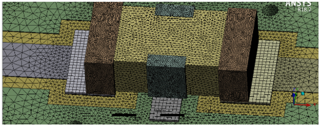
In addition, Mini-Circuits has developed market leading surface-mount package technologies employing both LTCC and organic substrate materials that demonstrate outstanding electrical performance up to 55GHz.
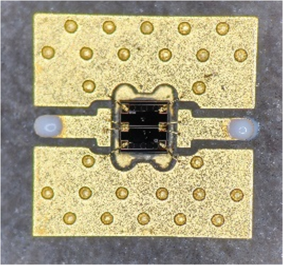
As a result of the technology break throughs, Mini-Circuits’ wide LTCC product portfolio offers our customers the following advantages:
- Reduced size and cost – most cost-effective solution in the mmWave frequency range.
- Part dimensions down to 0.02 x 0.02” footprint vs. 0.12 x 0.06”previously
- Superior RF performance in smaller size
- Ultra High Rejection Filters implemented
- Faster time to market for systems requiring custom components
- SIngle spin implementation enabling 4 months turnaround
Advanced Simulation and Modelling
The advanced performance modelling technologies used by Mini-Circuits allows successful design of LTCC parts up to 50GHz vs. typical limitation in the commercial market to <10GHz. The multi-physics simulation workflow employed by Mini-Circuits incorporates EM, structural and thermal simulators and each simulator factors in results from the other simulators to account for real-world physical effects.
Typically, Mini-Circuits combines two common simulation techniques to predict the RF performance of passive devices prior to their fabrication, each with its own pros and cons. The Method of Moments (MoM) technique works by meshing the conductive metallizations within the structure. This method is fast to perform and iterate but is mostly limited to 2D surfaces and assumes substrates extend infinitely in space, and hence it doesn’t provide a true substrate truncated 3D model.
The Finite Element Method (FEM) of simulation provides a true 3D model that allows us to truncate volumes. This method works by meshing the substrate structures rather than the conductors. FEM simulations better capture the coupling and parasitic effects through the substrate as well as the effects of truncating the 3D structure, all of which are absent in MoM. The drawback is that FEM simulations are typically slower to implement.
The FEM approach is more accurate for LTCC filters where the signal travels in a 3D fashion through a monolithic structure. Ideally, the characteristics of that structure would be uniform. However, in reality, LTCC structures consist of multiple layers of ceramic and conductive material with dispersive and anisotropic behavior. A true 3D characterization of the material is therefore required to account for the non-linear behavior of signals traveling through a structure with these properties.
While these two approaches are powerful, in the past they were incapable by themselves of achieving close agreement between simulation and measurement, and multiple design spins were still required. This limitation necessitated a deeper understanding of the material structure for its contributions to the real-world performance of the device. Mini-Circuits has extensively characterized the material properties of substrates and conductive elements used in LTCC products up to the millimeter wave range and integrated this know-how into a multi-physics simulation workflow.
Examples of Simulation vs. Measurement
Figure 3 shows a plot of S21 for an LTCC bandpass filter from a standard simulation model, Mini-Circuits’ advanced material simulation model, and actual measured performance. The pink plot represents the simulation results without the material knowledge we’ve modelled into newer simulations. Note the disparity between this simulation and the measured performance. The red line represents Mini-Circuits’ new simulation workflow incorporating all the material characterization and modelling we’ve conducted. Note that this simulation tracks the measured filter performance very closely across the full measured range.
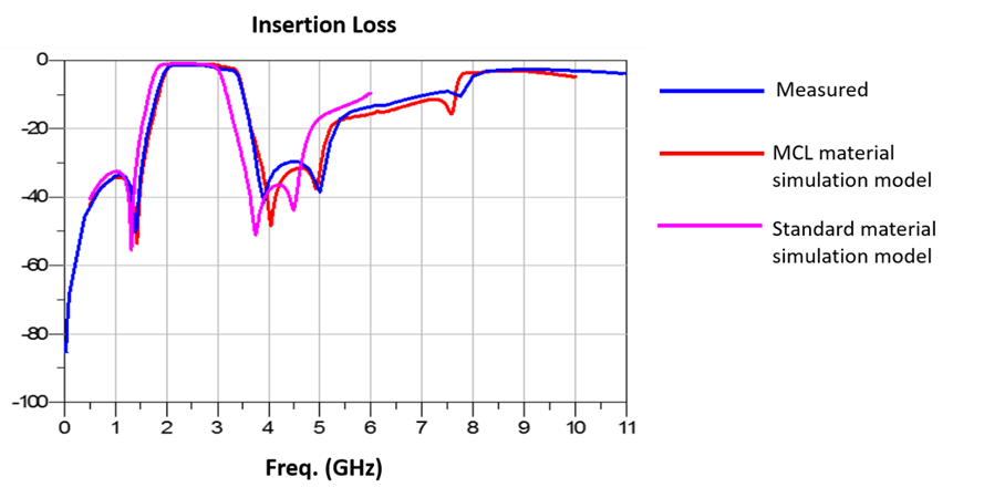
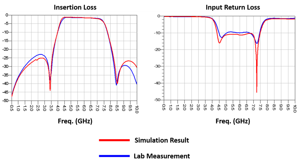
Figure 4 shows additional comparisons between Mini-Circuits’ advanced simulation results and measured performance for a different LTCC bandpass filter model. Both S21 and S11 are shown, illustrating highly accurate simulation results for both parameters. These cases are representative of the unique capability to achieve close agreement between simulation results and measured performance after the first run from the fab.
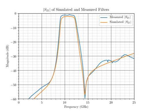
The learnings illustrated above were shown for LTCC filter designs utilizing lumped topologies, but the same approach has broad applicability for exploratory filter technologies as well such as distributed filter design shown in Figure 5.
The recent shift to applications at higher and higher frequencies has necessitated exploration of these distributed filter topologies. At Mini-Circuits’ we’ve taken many concepts from the research literature and created our own algorithm capable of synthesizing arbitrary distributed filter topologies based on our specifications. We’ve also created an optimization tool capable of producing simulated S-parameters and optimized dimensions on a full 3D model.
Conclusion
Single pass success has long been considered the ultimate goal in design workflows. The physically complex nature of LTCC technology makes it particularly challenging to achieve agreement between simulation and working design on the first try. By using extensive material characterization and modelling together with advanced design tools, proprietary algorithms, and our novel design workflow, our simulations now account for real-world effects on performance to the degree that we can consistently achieve first-spin success in LTCC designs. Our capabilities in this area have helped us accelerate standard and custom parts to reduce customers’ time to market. These innovations have also enabled us to enhance existing LTCC filter designs, reducing size and improving rejection performance. The design capability presented in this article extends to other technologies and innovations in high-frequency packaging solutions.
Mini-Circuits LTCC Filters Link
https://www.minicircuits.com/products/LTCC-Ceramic-RF-Filters.html
